- 您现在的位置:买卖IC网 > Sheet目录369 > W9725G6IB-25 (Winbond Electronics)IC DDR2-800 SDRAM 256MB 84-WBGA
W9725G6IB
7.3
7.3.1
Command Function
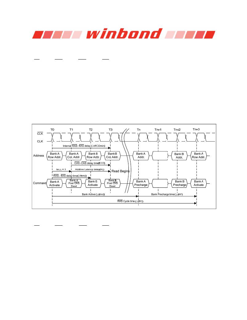
Bank Activate Command
( CS = "L", RAS = "L", CAS = "H", WE = "H", BA0, BA1 = Bank, A0 to A12 be row address)
The Bank Activate command must be applied before any Read or Write operation can be executed.
Immediately after the bank active command, the DDR2 SDRAM can accept a read or write command
on the following clock cycle. If a Read/Write command is issued to a bank that has not satisfied the
t RCDmin specification, then additive latency must be programmed into the device to delay when the
Read/Write command is internally issued to the device. The additive latency value must be chosen to
assure t RCDmin is satisfied. Additive latencies of 0, 1, 2, 3 and 4 are supported. Once a bank has been
activated it must be precharged before another Bank Activate command can be applied to the same
bank. The bank active and precharge times are defined as t RAS and t RP , respectively. The minimum
time interval between successive Bank Activate commands to the same bank is determined by the
RAS cycle time of the device (t RC ). The minimum time interval between Bank Activate commands is
t RRD .
Figure 12 — Bank activate command cycle: t RCD = 3, AL = 2, t RP = 3, t RRD = 2, t CCD = 2
7.3.2
Read Command
( CS = "L", RAS = "H", CAS = "L", WE = "H", BA0, BA1 = Bank, A10 = "L", A0 to A8 = Column
Address)
The READ command is used to initiate a burst read access to an active row. The value on BA0, BA1
inputs selects the bank, and the A0 to A8 address inputs determine the starting column address. The
address input A10 determines whether or not Auto-precharge is used. If Auto-precharge is selected,
the row being accessed will be precharged at the end of the READ burst; if Auto-precharge is not
selected, the row will remain open for subsequent accesses.
Publication Release Date: Oct. 23, 2009
- 20 -
Revision A04
发布紧急采购,3分钟左右您将得到回复。
相关PDF资料
W9725G6JB25I
IC DDR2 SDRAM 256MBIT 84WBGA
W9725G6KB-25I
IC DDR2 SDRAM 256MBIT 84WBGA
W972GG6JB-3I
IC DDR2 SDRAM 2GBITS 84WBGA
W9751G6IB-25
IC DDR2-800 SDRAM 512MB 84-WBGA
W9751G6KB-25
IC DDR2 SDRAM 512MBIT 84WBGA
W9812G6JH-6I
IC SDRAM 128MBIT 54TSOPII
W9816G6IH-6I
IC SDRAM 16MBIT 50TSOPII
W9825G6JH-6I
IC SDRAM 256MBIT 54TSOPII
相关代理商/技术参数
W9725G6JB
制造商:WINBOND 制造商全称:Winbond 功能描述:4M ? 4 BANKS ? 16 BIT DDR2 SDRAM
W9725G6JB-25
制造商:Winbond Electronics Corp 功能描述:DRAM Chip DDR2 SDRAM 256M-Bit 16Mx16 1.8V 84-Pin WBGA 制造商:Winbond Electronics 功能描述:512MB DDRII
W9725G6JB25I
功能描述:IC DDR2 SDRAM 256MBIT 84WBGA RoHS:是 类别:集成电路 (IC) >> 存储器 系列:- 标准包装:150 系列:- 格式 - 存储器:EEPROMs - 串行 存储器类型:EEPROM 存储容量:4K (2 x 256 x 8) 速度:400kHz 接口:I²C,2 线串口 电源电压:2.5 V ~ 5.5 V 工作温度:-40°C ~ 85°C 封装/外壳:8-VFDFN 裸露焊盘 供应商设备封装:8-DFN(2x3) 包装:管件 产品目录页面:1445 (CN2011-ZH PDF)
W9725G6KB-18
制造商:Winbond Electronics 功能描述:IC MEMORY 制造商:Winbond Electronics Corp 功能描述:IC MEMORY
W9725G6KB-25
功能描述:IC DDR2 SDRAM 256MBIT 84WBGA RoHS:是 类别:集成电路 (IC) >> 存储器 系列:- 标准包装:1 系列:- 格式 - 存储器:闪存 存储器类型:闪存 - NAND 存储容量:4G(256M x 16) 速度:- 接口:并联 电源电压:2.7 V ~ 3.6 V 工作温度:0°C ~ 70°C 封装/外壳:48-TFSOP(0.724",18.40mm 宽) 供应商设备封装:48-TSOP I 包装:Digi-Reel® 其它名称:557-1461-6
W9725G6KB-25 TR
制造商:Winbond Electronics Corp 功能描述:256M DDR2-800, X16
W9725G6KB25A
制造商:WINBOND 制造商全称:Winbond 功能描述:DLL aligns DQ and DQS transitions with clock, Data masks (DM) for write data, Write Data Mask
W9725G6KB25I
制造商:Winbond Electronics Corp 功能描述:DRAM Chip DDR2 SDRAM 256M-Bit 16Mx16 1.8V 84-Pin WBGA 制造商:Winbond Electronics 功能描述:IC DDR2 SDRAM 256M 2.5NS 84WBGA 制造商:Winbond Electronics Corp 功能描述:IC DDR2 SDRAM 256M 2.5NS 84WBGA 制造商:Winbond 功能描述:DRAM Chip DDR2 SDRAM 256M-Bit 16Mx16 1.8V 84-Pin WBGA
